The idea of ‘nanotechnology’ was kindled by a talk – There’s Plenty of Room at the Bottom – given by the famous physicist Richard Feynman at an American Physical Society meeting at CalTech back in 1959. In this talk, he described a possibility to manipulate and control individual atoms and molecules. Since then, brilliant minds have joined in this new area, creating many new devices to help understanding how things work at the atomic level and new ways to create functional materials with nanoscale accuracy. Along the way, Chinese scientists also have made their marks.
In the field of nanocharacterization, scientists at the Institute of Chemistry, CAS developed China’s first scanning tunneling microscope (STM) that integrates computer control, data analysis, and image processing, and China’s first atomic force microscope (AFM) in 1988, providing useful tools for China’s nanotechnology research. In 2001, scientists from the Chinese University of Science and Technology (CUST) obtained the C60 single-molecule image capable of resolving the chemical bonds of C-C and C=C for the world’s first time using a low-temperature STM.
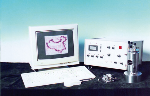
China’s first atomic force microscope (AFM) developed by the Institute of Chemistry, CAS (Credit: CAS)
Raman Imaging Breaks the Nanometer Barrier
Later in 2013, CUST scientists also made a great breakthrough in how to gain a clearer view of tiny molecules, which won the Outstanding Scientific and Technological Achievement Award of the Chinese Academy of Sciences in 2014.
To get a glimpse of tiny molecules usually depends on the use of Raman spectroscopy, which relies on a phenomenon that photons from a light shone on a molecule interact with bonds within molecules or materials. As a result, the frequency of these photons could be shifted, providing a characteristic fingerprint of the molecule’s structure. It was also demonstrated that such Raman effect can be boosted when molecules are adsorbed to metallic nanoparticles because of the involvement of plasmons – electronic oscillations at the surface of metals.

Zoom in on single molecules by new Raman spectroscopy under carefully controlled conditions. (Credit: USTC)
Then another brilliant idea kicked in by using the tip of an atomic force microscope as a single, highly focused metallic surface. When it is brought to within a few nanometres of the sample under investigation, plasmonic excitation effectively creates a single hotspot of surface-enhanced Raman scattering, a method called tip-enhanced Raman scattering, or TERS. This has allowed Raman scattering to reach a resolution of around 10nm.
In 2013, DONG Zhenchao, HOU Jianguo, and coworkers at the USTC successfully broke the nanometer barrier of Ramon imaging, making its imaging spatial resolution reach 0.5 nanometers. This method would even allow scientists to identify the structure inside the molecules. The findings were published in the journal of Nature (2013, doi: 10.1038/nature12151).
“The method would be useful in photonics to study the activity of biomolecules and cells. Other applications could include catalysis, molecular electronics, and other fields where single-molecule resolution is important,” as stated by Dong.
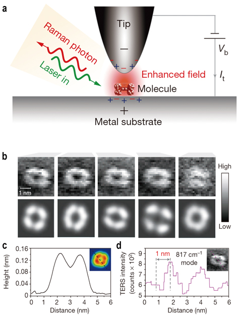
a, Schematic tunneling-controlled TERS in a confocal-type side-illumination configuration, in which Vb is the sample bias and It is the tunneling current. A sample molecule is trapped within a cavity between a metal surface and the tip of the STM probe. Shining laser light on the sample results in Raman scattering from the molecule. It also creates waves of oscillating electrons known as a plasmon on the metal surface. The researchers tune the plasmon so that it is in resonance with both the laser light and the frequency of the Raman emission modes. That double resonance boosts the Raman signal to achieve spatial resolution better than 1 nm. b, The top panels show experimental TERS mapping of a single molecule for different Raman peaks. The bottom panels show the theoretical simulation of the TERS mapping. c, Height profile of a line trace in the inset STM topograph. d, TERS intensity profile of the same line trace for the inset Raman map. (Credit: Nature)
As noted by a commentary on this work in the same issue (Nature 2013, doi: 10.1038/498044a), “Optical spectroscopic imaging has taken a leap into the intramolecular regime with an approach that achieves subnanometre spatial resolution…. The authors’ work opens up avenues for probing and even controlling materials on molecular scales.”
Visualizing Hydrogen Bonds
In 2013, scientists from the CAS National Center for Nanoscience and Technology (NCNST) reported a real-space visualization of the formation of intermolecular hydrogen bonds with AFM technology (Science 2013, doi: 10.1126/science.1242603). This is the first ever sight of hydrogen bonds, providing the first intuitive evidence for the “essence of hydrogen bonding” that has been debated in the chemical community for more than 80 years.
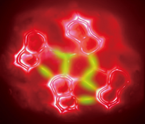
An art illustration based on the AFM measurement of a 8-hq assembled cluster on Cu(111) with the possible hydrogen bonds illuminated in green. (Credit: NCNST)
The established technique has broad application prospects in the study of intermolecular interactions. “The hydrogen bonding is ubiquitous in nature and central to biological functions, the present technique may provide an important and complementary characterization method for unraveling the fundamental aspects of molecular interactions at the single-molecule level. The observation of hydrogen bonding in real-space may also stimulate theoretical discussion about the nature of this intermolecular interaction,” as stated by the authors of this work.
In the field of creating new nanomaterials and devices, the CAS Institute of Physics (IOP) and the CAS Institute of Metal Research (IMR), etc. made numerous advances in the preparation of carbon nanotubes, nanostructures and surfaces with controlled properties in the last two decades.
After long-lasting efforts, scientists at the CAS Institute of Chemistry developed a complete industrial chain for nano-green printing, and established nanomaterial-based green platemaking technology in 2016, which could greatly reduce the chemical pollutants made by traditional platemaking.
New Alloy Design Enables Subnanosecond Memory Writing
Operation speed is a key challenge in phase-change random-access memory (PCRAM) technology, especially for achieving subnanosecond high-speed cache memory. Commercialized PCRAM products are limited by the tens of nanoseconds writing speed, originating from the stochastic crystal nucleation during the crystallization of amorphous germanium antimony telluride (Ge2Sb2Te5, GST).
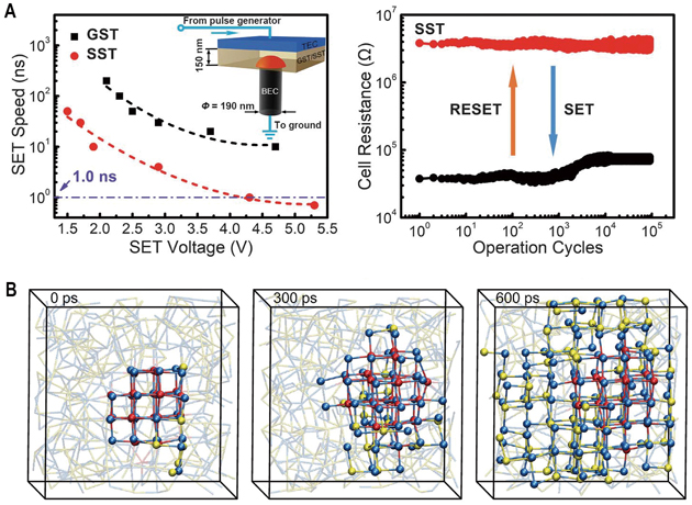
A and B, Demonstration of 0.7-ns high-speed writing device. C, Simulated crystallization mechanism of the novel samarium antimony tellurium (Sc-Sb-Te, STT) phase changing materials. (Credit: SIM)
Things changed in 2017. Scientists at the Shanghai Institute of Microsystem and Information Technology (SIM), CAS together with their collaborators demonstrated an alloying strategy to speed up the crystallization kinetics. They designed a scandium antimony telluride (Sc0.2Sb2Te3, SST) compound that allows a writing speed of only 700 picoseconds without preprogramming in a large conventional PCRAM device (Science 2017, doi: 10.1126/science.aao3212). This achievement holds great significance for China to independently develop memory chips.
In the field of nano-catalysis, CAS scientists also made many groundbreaking contributions, among which the original concepts of single-atom catalysis and confinement effects on catalysis stand out.
Single-Atom Catalysis
Catalysts are agents that boost the speed of chemical reactions while undergoing no permanent change themselves. They play a very important role in industrial production. How to improve the efficiency of catalysts and thus promote the development of industrial production is an important subject pursued by scientists.
Most of the catalytic reactions involved in current industrial production are heterogeneous catalysis that happens at the interface (e.g., solid-liquid or solid-gas interface) of two different phases. Heterogeneous catalytic reactions usually occur on the catalyst surface. In order to improve the efficiency of the catalysts, scientists come up with many ways to “break up” these catalysts and let the dispersed catalyst particles contact as much as possible with the reactants. The catalytic nanoparticles are the result of this effort.
However, catalytic nanoparticles suffer from instability. These tiny particles would aggregate and become inactive at high temperatures.
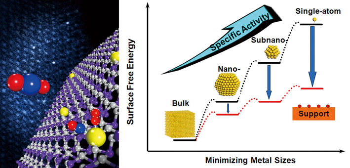
Left: an art illustration of single platinum atoms (yellow balls in the model) on iron oxide (purple and gray) mediate conversion of CO to CO2 with extremely high atom efficiency and stability. Right: the dispersion of single-atom catalysts on supports shows many unique characters that enable both improve the catalytic specificity and activity. (Credit: DICP)
Scientists are a bunch of people who are good at solving problems and they come up with another idea by allocating the catalytic particles to some supporting materials so that the catalytic particles would not come together and lose their activity. Because the catalytic particles are fixed at their so-called “working positions”.
It seems that science is indeed a way of refreshing our appreciations of how things work. In this case, the supporting materials that once be considered to merely provide working positions for the catalytic particles turn out to be relevant in tuning the characters of the allocated catalysts, as well as their work efficiency in catalysis.
Scientists also found that most of the catalytic reactions happen at the sites where the catalytic particles contact with the supporting materials. The catalytic particles work together with the supports to make a catalytic reaction possible; while the particles away from the supports are not making much contribution to catalysis.
To make the catalytic particles contact as much as possible with the supports, scientists attempt to break up the catalytic particles to single atoms so that each one could make a direct contact with the supports – “each one is working”, so to speak. Though the idea seems alluring, the act to disperse catalysts to a single-atom scale is quite challenging.
In 2011, scientists led by ZHANG Tao from the CAS Dalian Institute of Chemical Physics (DICP), together with collaborators from Tsinghua University and University of Missouri-St Louis made the first breakthrough. They revealed that single platinum atoms (yellow balls in the model and three bright spots in TEM image) on iron oxide (purple and gray) mediate conversion of CO to CO2 with extremely high atom efficiency and stability (Nature Chemistry 2011, doi: 10.1038/nchem.1095). This successful demonstration has ushered in a new field known as “single-atom catalysis”, which had drawn a lot of brilliant minds into this field since then. “The work may lead to low-cost industrial catalysts and addresses questions in fundamental catalytic science,” commented by Chemical & Engineering News (C&EN).
The Direct Conversion of CH4
In 2014, scientists at the CAS Dalian Institute of Chemical Physics (DICP) reported that single iron sites embedded in a silica matrix enable direct, nonoxidative conversion of methane, exclusively to ethylene and aromatics (Science 2014, doi: 10.1126/science.1253150). This so-called confinement effects on catalysis can also be extended to other circumstances, including space confinement and interface confinement.

Direct conversion of CH4 to ethylene and aromatics with lattice-confined single iron sites embedded within a silicide matrix. (Credit: DICP)